The semiconductor industry has become essential to the modern global economy. Advanced chips support artificial intelligence, smartphones, cloud computing, vehicles, industrial equipment, and many digital services. As demand for powerful computing grows, governments and technology companies are paying closer attention to where important semiconductors are manufactured.
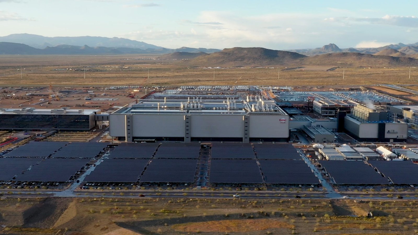
TSMC Arizona has become a major part of this discussion in the United States. Taiwan Semiconductor Manufacturing Company selected Phoenix for an advanced semiconductor manufacturing site and has steadily expanded its plans. What started as a $12 billion project has developed into a much larger investment strategy focused on chip production, advanced packaging, research, jobs, and semiconductor supply chain growth.
People searching this keyword usually want information about the Phoenix fabs, investment value, production technology, construction progress, careers, and importance of the project. This guide explains the Arizona expansion and why it matters to the American and global technology industries.
What Is TSMC Arizona
TSMC Arizona refers to Taiwan Semiconductor Manufacturing Company’s advanced semiconductor manufacturing operations in Phoenix, Arizona. The company announced its original Arizona project in 2020 and selected Phoenix for its first advanced semiconductor manufacturing site in the United States.
The project has expanded considerably. TSMC now describes an Arizona vision that includes six semiconductor wafer fabrication plants, two advanced packaging facilities, and a research and development team center.
| Topic | Key Information |
|---|---|
| Company | Taiwan Semiconductor Manufacturing Company |
| Location | Phoenix, Arizona |
| Original announcement | 2020 |
| Planned investment | $165 billion |
| Planned wafer fabs | Six |
| Packaging facilities | Two |
| Additional facility | R&D team center |
| Main industry | Semiconductor manufacturing |
The scale of the project has made Phoenix an important location in discussions about advanced chip manufacturing and American technology infrastructure.
Why TSMC Selected Arizona
Arizona has developed a growing semiconductor and advanced manufacturing ecosystem. The state offers industrial land, engineering talent, technology operations, and connections with companies involved in the semiconductor supply chain.
A semiconductor fab requires significant space and specialized infrastructure. Production facilities need highly controlled environments, advanced equipment, electricity, water systems, and trained employees.
Phoenix also provides a strategic location for a large manufacturing campus. Many major customers served by TSMC are American technology companies, so expanding production in the United States can support geographic diversification.
Federal semiconductor policy has also encouraged domestic manufacturing investment. Government support through the CHIPS and Science Act has become an important part of the broader Arizona project.
The location decision is therefore connected with customer demand, supply chain strategy, manufacturing capacity, and long-term semiconductor industry growth.
How the Arizona Investment Expanded
TSMC originally announced a $12 billion investment in Phoenix in May 2020. The project later expanded as demand for advanced chips and concerns about semiconductor supply chains increased.
Plans grew to more than $65 billion for three advanced fabs. TSMC then announced an additional $100 billion U.S. investment commitment in 2025, bringing its planned total investment to $165 billion.
The expanded vision includes three additional fabs, two advanced packaging facilities, and a research and development team center.
This means TSMC Arizona is no longer simply a single semiconductor factory. The company is developing a large manufacturing cluster intended to support advanced chip production over the long term.
Projects of this scale are completed in stages. Construction, equipment installation, worker training, process qualification, and customer production requirements can take years before a fab reaches full manufacturing activity.
The First Phoenix Fab
The first Arizona fab represents an important milestone for advanced semiconductor manufacturing in the United States. TSMC has reported that the facility entered high-volume production in the fourth quarter of 2024.
The fab uses N4 process technology. Advanced semiconductor manufacturing at this level is relevant to high-performance computing, artificial intelligence, and other demanding technology applications.
Producing modern chips is extremely complex. Semiconductor wafers pass through many carefully controlled manufacturing steps. Small process variations can influence performance and production yield.
Completing a fab building is only one part of the process. Manufacturing equipment must be installed, production systems tested, employees trained, and processes qualified.
The first fab established an operating manufacturing base for the larger Phoenix campus. Its production progress is important because future Arizona facilities are expected to introduce additional advanced semiconductor technologies.
Fab 2 and Advanced Semiconductor Technology
The second Arizona fab is designed to expand the site’s manufacturing capabilities. TSMC has connected the facility with N3 and more advanced process technologies.
Advanced semiconductor processes can support improved performance, energy efficiency, and transistor density. These characteristics are increasingly important for AI systems and high-performance computing products.
The second fab demonstrates that the Phoenix campus is intended to progress beyond one generation of semiconductor technology.
Semiconductor production schedules can depend on construction progress, equipment availability, technology development, and customer demand. A large fab must complete several technical stages before reaching high-volume manufacturing.
As demand for advanced computing continues, manufacturing capacity has become strategically important for technology companies.
Fab 2 forms a major part of TSMC’s plan to build a larger leading-edge semiconductor cluster in Arizona rather than operating only one advanced manufacturing facility.
Fab 3 and Two Nanometer Plans
The third Phoenix fab is another important part of the TSMC Arizona expansion. In May 2026, the facility reached its topping-out milestone, marking the installation of the final and highest structural beam.
Fab 3 is planned to use highly advanced two nanometer process technology.
Two nanometer manufacturing is significant because the semiconductor industry continues to improve chip performance and energy efficiency. Advanced process technologies can support future AI, data center, and high-performance computing systems.
A topping-out ceremony does not mean semiconductor production can begin immediately. The facility still requires extensive internal work, cleanroom preparation, equipment installation, and manufacturing qualification.
However, the construction milestone shows continued progress at the Phoenix campus.
Fab 3 also highlights the long-term nature of the Arizona project. TSMC is preparing the site for increasingly advanced generations of semiconductor manufacturing.
Why TSMC Arizona Matters for AI
Artificial intelligence has become a major source of semiconductor demand. Training and running sophisticated AI systems requires powerful computing infrastructure supported by advanced processors.
TSMC operates as a semiconductor foundry. Technology companies design chips, while TSMC provides specialized manufacturing capabilities needed to produce them.
This business model makes the company’s manufacturing capacity important to the wider AI industry.
The Arizona expansion can provide advanced manufacturing capacity in the United States and support customers seeking more geographically diverse semiconductor production.
AI is not the only market connected with the project. Advanced chips are also used in smartphones, vehicles, high-performance computers, and connected devices.
However, rapid AI investment has increased attention on chip manufacturing. The Phoenix campus is increasingly viewed as part of the physical manufacturing infrastructure supporting future computing technology.
Jobs and Workforce Development
Large semiconductor projects create demand for a wide range of workers. Government project information estimates that the first three Arizona fabs will support approximately 6,000 direct manufacturing jobs and more than 20,000 total unique construction jobs during the decade.
Semiconductor manufacturing requires engineers, equipment technicians, process specialists, facilities teams, IT professionals, quality workers, and safety staff.
Fab construction also requires specialized trades. Semiconductor facilities contain complex electrical, water, ventilation, and cleanroom systems that must meet strict manufacturing requirements.
Workforce development is therefore an important challenge for TSMC Arizona. Building advanced facilities is not enough. The company also needs trained employees capable of operating and maintaining semiconductor production systems.
The project may encourage universities, colleges, and technical training organizations to expand semiconductor-related education and workforce programs in Arizona.
CHIPS Act Support
The CHIPS and Science Act was designed partly to encourage semiconductor manufacturing investment in the United States. The Arizona project became one of the major advanced manufacturing developments supported through the program.
The U.S. Department of Commerce awarded TSMC Arizona up to $6.6 billion in direct funding for its leading-edge Phoenix manufacturing plans.
Government officials have connected semiconductor investment with economic and national security. Advanced chips support AI, computing, automotive technology, consumer electronics, and other important industries.
Global supply disruptions also increased interest in expanding American semiconductor manufacturing capacity.
Government incentives do not remove the technical or financial challenges of building fabs. Semiconductor facilities remain extremely expensive and complex.
However, public support can influence where companies make major long-term investments and can help develop broader manufacturing ecosystems around large semiconductor projects.
Advanced Packaging and Research Facilities
The expanded Arizona plan goes beyond wafer fabrication. TSMC has also announced two advanced packaging facilities and a research and development team center.
Advanced packaging is becoming increasingly important in modern semiconductor technology. Complex computing products may combine several chip components within sophisticated packages.
This is particularly relevant to AI and high-performance computing. Advanced packaging can help connect processors, memory, and other components efficiently.
Adding packaging facilities can support a more complete semiconductor ecosystem around the Phoenix manufacturing campus.
The planned research and development presence is also significant. Semiconductor manufacturing and technology development are closely connected.
Together, fabs, packaging operations, and research activities can create a broader technology cluster. This approach is different from operating a single factory focused on one production stage.
Water and Infrastructure Questions
Water use is frequently discussed in relation to semiconductor manufacturing in Arizona. Chip production requires highly purified water during several manufacturing processes.
Arizona’s dry climate makes industrial water management an important public topic.
Modern semiconductor facilities can use recycling and conservation systems, but large manufacturing projects still require careful infrastructure planning.
Electricity is another major consideration. Advanced fabs operate complex production tools and tightly controlled manufacturing environments.
Transportation, supplier access, and construction capacity are also necessary for a large semiconductor campus.
As the Phoenix site expands, infrastructure management will remain an important issue for TSMC, local officials, and surrounding communities.
Public discussion should focus on verified project information and actual resource planning rather than assuming that every semiconductor facility operates in exactly the same way.
Semiconductor Supply Chain Importance
Advanced semiconductors are essential to modern economies. Chip shortages can affect technology businesses, vehicle manufacturers, communication systems, and industrial companies.
A significant amount of leading-edge semiconductor production has historically been concentrated in Asia. This geographic concentration has increased concern about supply chain resilience.
The Arizona project does not replace TSMC’s major manufacturing operations in Taiwan. Instead, it adds advanced production capacity in another location.
Geographic diversification can provide additional manufacturing options and support U.S. efforts to strengthen domestic semiconductor capacity.
National security discussions also focus on access to advanced chips because computing technology supports economic and strategic systems.
For this reason, TSMC Arizona is more than a Phoenix construction project. It has become part of a wider discussion about technology manufacturing, supply chain resilience, and access to advanced semiconductor production.
Economic Impact on Phoenix
A planned $165 billion investment can influence the regional economy in several ways. Direct manufacturing employment represents only one part of the possible impact.
Construction businesses, engineering firms, equipment suppliers, logistics companies, and service providers may benefit from semiconductor development.
The presence of a major manufacturing campus can also encourage suppliers to establish operations nearby. Semiconductor companies often benefit from close access to customers and technical support.
New employment can increase demand for housing, transportation, and local services.
Rapid growth can also create challenges. Housing affordability, infrastructure capacity, and workforce competition may require attention as the semiconductor ecosystem expands.
The long-term economic impact will depend on the development of the fabs, supporting businesses, and Arizona’s ability to train enough skilled workers for advanced manufacturing roles.
Careers at the Phoenix Campus
Career searches are another reason people research TSMC Arizona. The company continues to advertise positions connected with its Phoenix operations.
Job categories can include engineering, facilities, construction, manufacturing programming, safety, quality, information technology, and administrative work.
Requirements vary by position. Some jobs need specialized engineering education or semiconductor experience. Technician, support, and corporate roles can have different qualification requirements.
Applicants should review current official career information because available positions change as facilities move through construction and manufacturing stages.
Job seekers should also read individual descriptions carefully. Not every position involves direct chip production.
As the Arizona campus expands, workforce requirements are likely to continue changing. New fabs, packaging facilities, and other operations can create different hiring needs throughout the development of the project.
Challenges Facing the Arizona Expansion
Building leading-edge semiconductor fabs is difficult. TSMC must manage construction, equipment installation, workforce development, suppliers, manufacturing qualification, and operating costs.
Workforce availability has received particular attention because advanced semiconductor production requires specialized skills and strict manufacturing processes.
The company must also coordinate technology plans with customer demand. Semiconductor markets can change as AI investment, consumer demand, and economic conditions shift.
Construction and operating costs in the United States can differ from established semiconductor manufacturing regions in Asia.
Despite these challenges, the project has progressed from an initial announcement to high-volume production at the first fab and continued development of additional facilities.
The long-term success of the campus will depend on manufacturing performance, skilled workers, customer demand, and the growth of a supporting semiconductor ecosystem in Arizona.
Final Thoughts
TSMC Arizona has developed from a $12 billion Phoenix fab announcement into a planned $165 billion semiconductor expansion. The current vision includes six wafer fabs, two advanced packaging facilities, and a research and development team center.
The first fab has entered high-volume production, while additional facilities are planned around increasingly advanced process technologies. Fab 3 has also reached an important construction milestone as the company develops its two nanometer manufacturing plans.
The project matters because advanced semiconductors support artificial intelligence, high-performance computing, vehicles, and many modern technologies. It also creates employment and contributes to U.S. semiconductor supply chain development.
For people researching TSMC Arizona, the main story is continued expansion. Phoenix is becoming an increasingly important location in the global advanced semiconductor manufacturing network.
Frequently Asked Questions
What is TSMC Arizona?
TSMC Arizona is Taiwan Semiconductor Manufacturing Company’s advanced semiconductor manufacturing operation and expanding fab campus in Phoenix.
How much is TSMC investing in Arizona?
TSMC has announced a planned $165 billion investment connected with its expanded U.S. semiconductor manufacturing strategy.
How many TSMC fabs are planned in Arizona?
The company’s current announced Arizona vision includes six semiconductor wafer fabrication plants.
What technology does the first Arizona fab use?
The first Phoenix fab entered high-volume production using TSMC’s N4 process technology.
Why is the Arizona project important?
The project supports advanced U.S. chip manufacturing, AI infrastructure, skilled employment, semiconductor supply chain diversification, and wider technology investment.
Read More: Augmented Reality (AR) Transforming the Way We Interact With the World